A Throughput-Optimized FPGA Architecture for Goldilocks NTT
We present a modular, fully-pipelined FPGA architecture for large NTT computations in the 64-bit Goldilocks finite field

3/22/23

Irreducible Team
Introduction
A key performance bottleneck in the computation of zero-knowledge succinct proofs (ZKPs) is the number-theoretic transform (NTT). The NTT is necessary for fast implementation of polynomial multiplication and Reed–Solomon encoding, which are used in many ZKP constructions.
In this post we present a modular, scalable, and fully-pipelined FPGA architecture for large NTT computations over the 64-bit Goldilocks finite field (GL64).
Modular: Any length of NTT computation can be decomposed into three basic building blocks: sub-NTTs (length of 8, 16, 32), twiddle factor multipliers, and transpose modules.
Scalable: This architecture can be easily extended to support larger NTTs. For example, a size-2¹² NTT can be extended to a size-2²⁴ NTT by composing multiple instances.
Fully-pipelined: The FPGA receives and transmits data without stalls caused by data dependencies. Data is continuously streamed and the modules achieve 100% throughput utilization.
NTT Background
The NTT is a linear transformation analogous to the discrete Fourier transform, but defined over finite fields rather than the complex numbers. When the field contains nᵗʰ roots of unity, the NTT can be performed efficiently on vectors of length n using the fast Fourier transform technique. In application, the NTT is used to convert degree n – 1 polynomials in coefficient form into evaluation form on the nᵗʰ roots of unity.
Denote ω for a primitive nᵗʰ root of unity, then the NTT of vector a is:
$$\begin{equation*}\begin{split} NTT_{\omega}(a)= \left( \sum_{j=0}^{n-1}a_{j} \omega^{ij} \right)_i \end{split}.\end{equation*}$$
The inverse transformation (INTT) transforms polynomials in evaluation form to coefficient form, and is computed with nearly the same complexity as the forward transformation:
$$\begin{equation*}\begin{split} INTT_{\omega}(\hat{a})= \left( \frac{1}{n} \sum_{j=0}^{n-1}\hat{a}_{j} \omega^{-ij} \right)_i = \frac{1}{n} NTT_{\omega^{-1}}(\hat{a}) \end{split}.\end{equation*}$$
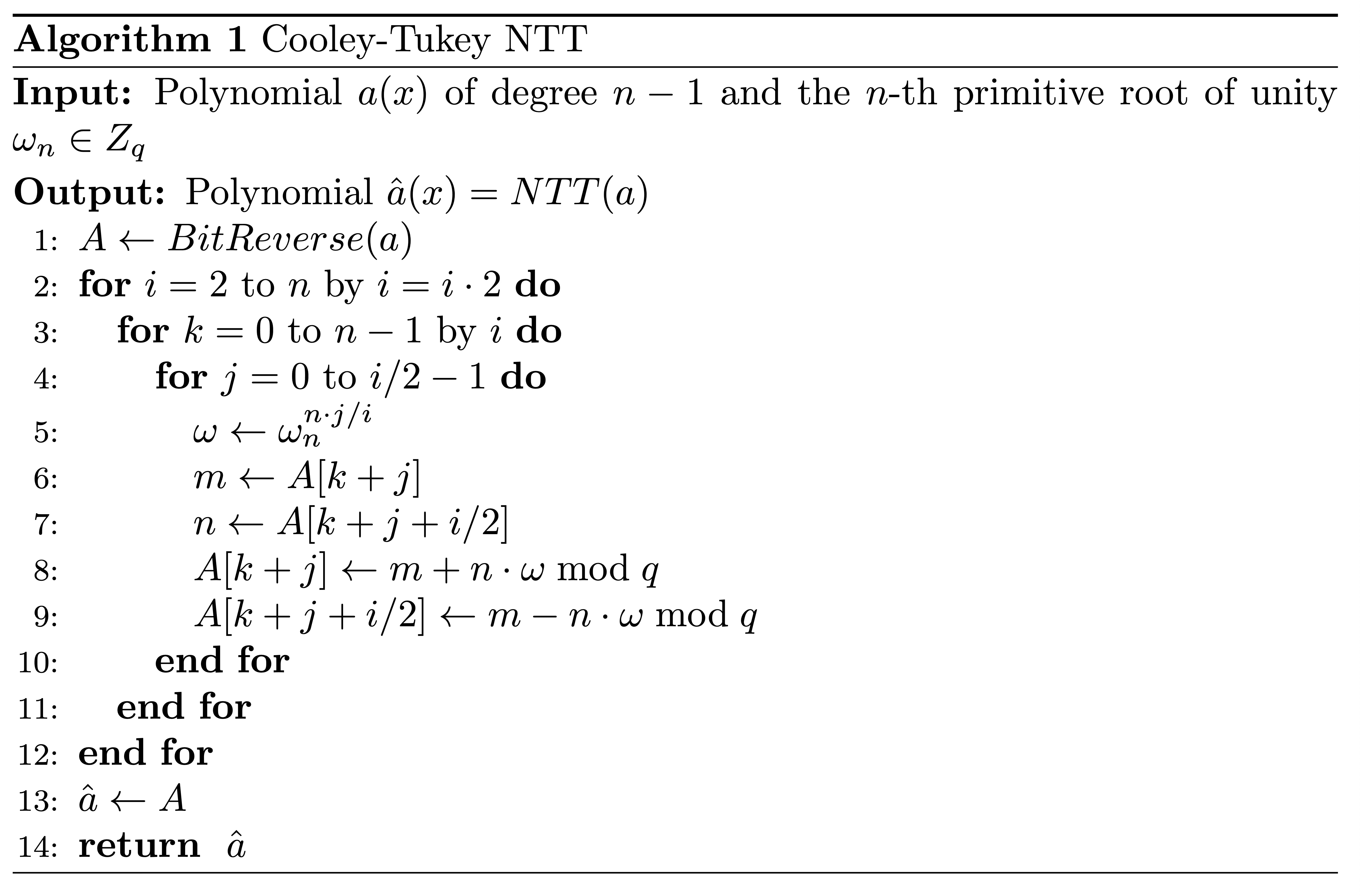
Cooley–Tukey NTT Algorithm
The most famous algorithm for fast Fourier transforms and NTT is Cooley–Tukey algorithm. This method leverages the symmetries of the nᵗʰ roots of unity to compute the transformation in a logarithmic number of loops over the vector. The Cooley–Tukey radix-2 NTT presented in Algorithm 1 has three layers of loops; the computation steps that comprise the inner loop are known as butterfly operations due to their associated patterns of data access. The butterfly operations have poor data locality in the later rounds of the outer loop, making this method efficient only for small instances.
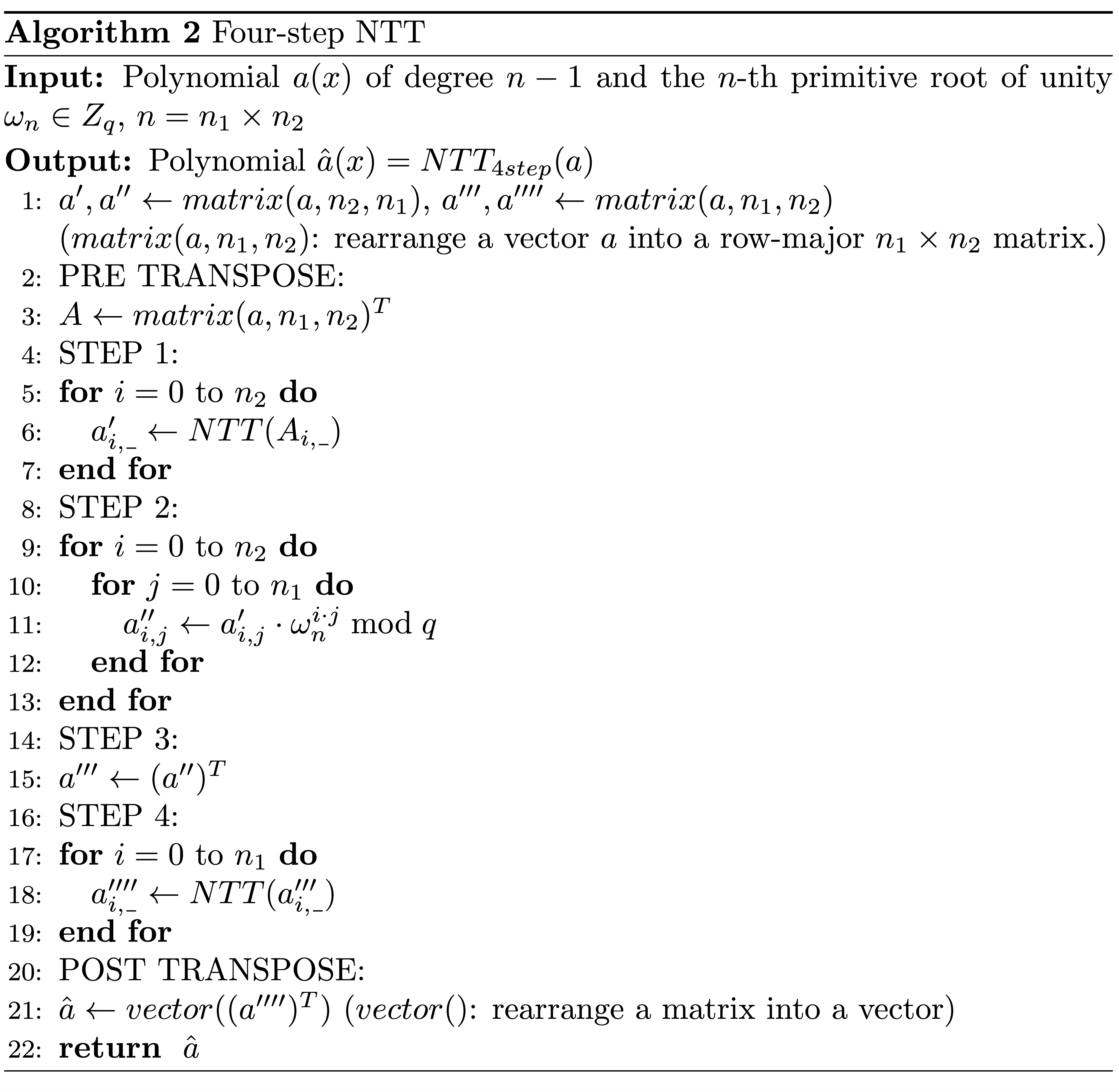
Four-Step NTT Algorithm
The four-step NTT algorithm was designed to overcome the limitations of the Cooley–Tukey algorithm on large vectors, like those required for ZKP computation. The algorithm starts by reshaping the n-length vector into an n₁ × n₂ matrix in column-major order, followed by four steps:
Compute the n₁ -length NTT over each of the n₂ rows.
Multiply element-wise by twiddle factors.
Transpose the matrix.
Compute the n₂ -length NTT over each of the n₁ rows.
By breaking one large NTT computation into a series of smaller NTTs and performing a single data transposition step, the four-step NTT has a far more manageable data access pattern than Cooley–Tukey over large vectors. The four-step NTT is shown in detail below in Algorithm 2.
Goldilocks Finite Field
GL64 is the prime field of size \(q = 2^{64} - 2^{32} + 1\), which has order-2³² roots of unity and several structural properties that make it efficient for modular arithmetic and NTTs. For this reason, GL64 has been adopted in several ZKP systems, notably the zkEVM, Plonky2, and Starky projects from 0xPolygon.
We observe here some useful identities on the powers of \(\phi = 2^{32}\) in the GL64 field, expressing the prime as \(q = \phi^2 - \phi + 1.\) It is easily shown that:
$$\begin{align}\phi^2 \equiv \phi - 1 &\mod q, \\\phi^3 \equiv -1 &\mod q.\end{align}$$
System Design
Our system architecture is co-designed holistically, bringing together:
Full-bandwidth communication between CPU host and FPGA accelerator over PCIe Gen4.
Flexible composition of NTT modules with a recursive N-step NTT algorithm.
Low-complexity modular arithmetic over GL64.
The fully-pipelined architecture is designed around the bandwidth bottleneck of 128 Gbps at the PCIe interface between the CPU host and the FPGA. At a clock frequency of 250 MHz, the NTT pipeline accepts 512 bits per cycle from the AXI4-Stream interface, containing 8 GL64 elements.
System-Level Integration
The computation starts with the user space application which generates the data payloads, in our case a ZKP application. We expose an API to the application for offloading NTT computations to the FPGA. The acceleration service exposed via this API transfers NTT input payloads to the FPGA and receives results over the PCIe Gen4 x8 lanes interface, framing packets with the maximum TLP size of 4 kB. The service sits atop the Data Plane Development Kit (DPDK) poll-mode driver, enabling kernel bypass for performance efficiency on the data path. Dedicated writer and reader threads are spinning on isolated CPU cores. The writer thread is responsible for dispatching computation requests and sending them through via the TX queues to the FPGA, and the reader continuously polls RX queues, collecting results from the FPGA and providing them up the stack to the user application.
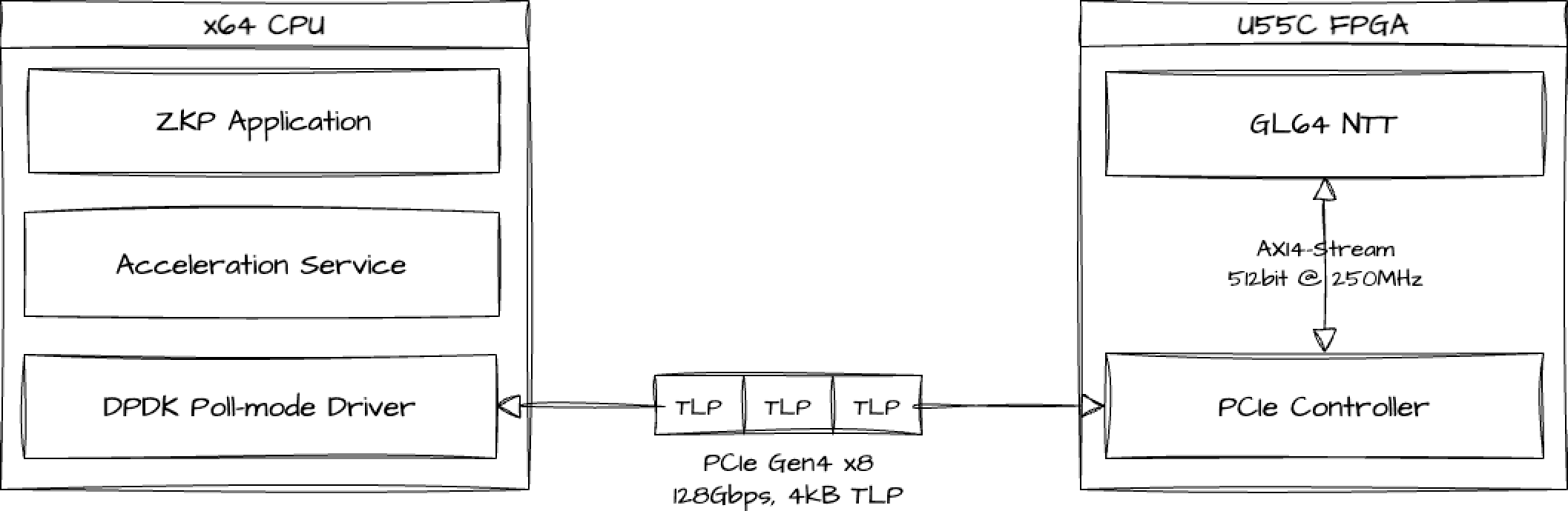
Figure 1. System-Level Integration.
Modular Arithmetic in GL64 Finite Field
The Goldilocks primes are structured to bolster computational efficiency in two ways:
being Karatsuba-friendly, and
allowing efficient modular reduction.
Using the identity \(\phi^2 \equiv \phi - 1 \mod q\) from Equation (1), we derive a simplified Karatsuba multiplication formula:
$$\begin{align*}a b &\equiv (a_0 + a_1\phi)(b_0 + b_1\phi) &\mod q, \\ &\equiv a_0b_0 + (a_0b_1 + b_0a_1)\phi + a_1b_1\phi^2 &\mod q, \\ &\equiv (a_0b_0 - a_1b_1) + ((a_0 + a_1)(b_0+b_1) - a_0b_0)\phi &\mod q. \end{align*}$$
Observe that the value \(c \equiv (a_0b_0 - a_1b_1) + ((a_0 + a_1)(b_0 + b_1) - a_0b_0)\phi\) is 98 bits wide. We can then complete the modular reduction with no further multiplications using the identities from Equation (2). The value \(c\) is split into four 32-bit words c₀, c₁, c₂, c₃, where c₃ is only 2 bits wide, and further reduced as follows:
$$\begin{align*} ab &\equiv c &\mod q, \\ &\equiv c_0 + c_1\phi + c_2\phi^2 + c_3\phi^3 &\mod q, \\ &\equiv c_0 + c_1\phi + c_2(\phi - 1) - c_3 &\mod q, \\ &\equiv c_0 - c_2 - c_3 + (c_1 + c_2)\phi &\mod q. \end{align*}$$
Combining these steps together, we get the GL64 modular multiplier architecture shown below:
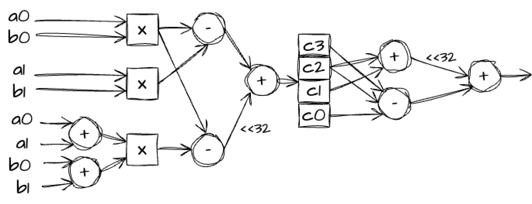
Figure 2. GL64 Modular Multiplier Architecture.
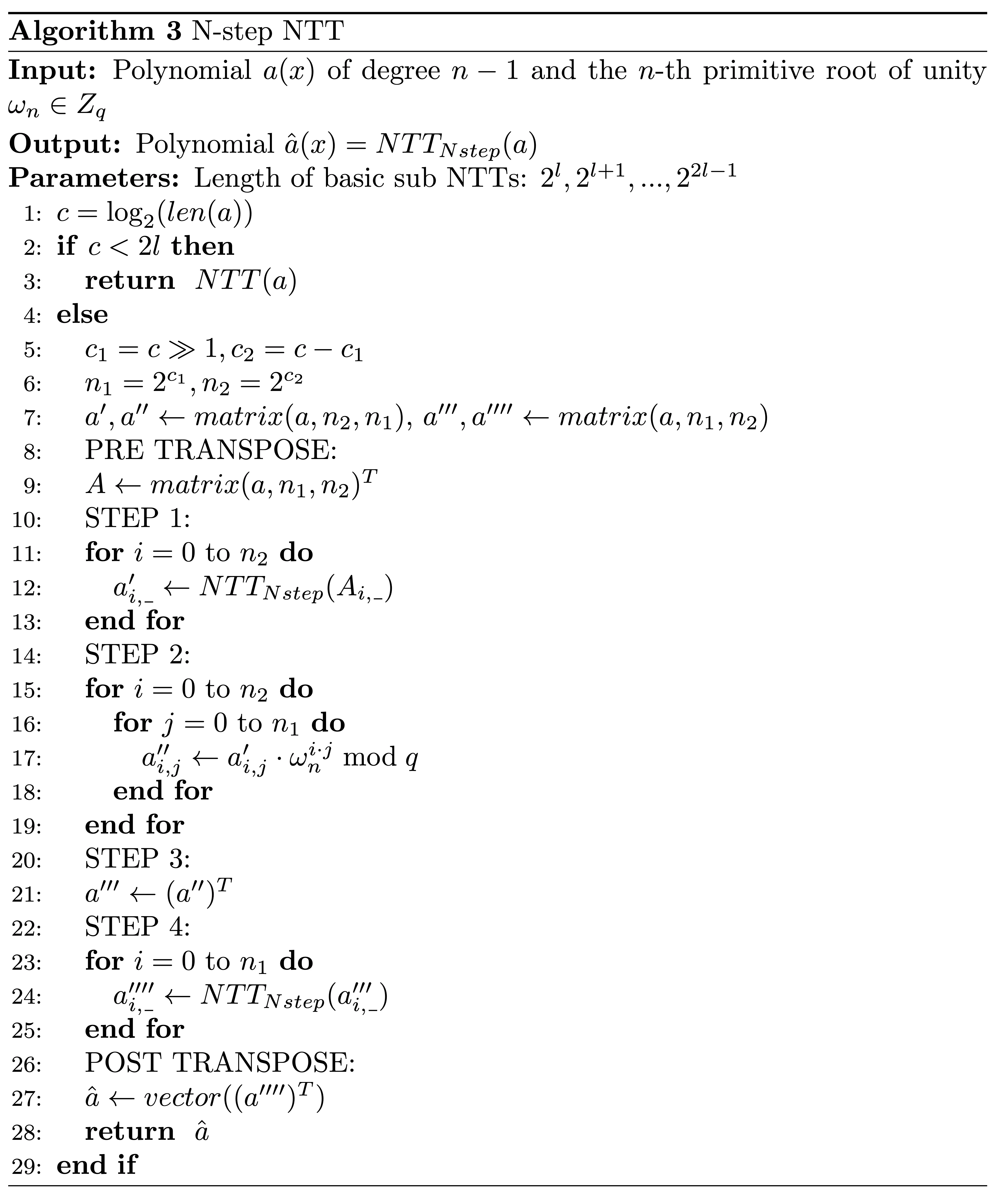
Recursive N-step NTT
The four-step NTT algorithm can be computed recursively, further decomposing the NTT operations in Steps 1 and 4 of Algorithm 2. In this manner, we can split a large NTT into a series of sub-NTTs of a base size \(2^l\). This technique, which we call the N-step NTT algorithm (\(NTT_{Nstep}\)), is suitable for fully-pipelined hardware implementations sustaining a throughput of \(l\) elements per cycle and leads to modular designs that scale to larger NTT sizes.
Sub-NTT Architecture
At each clock cycle (4 ns at 250 MHz clock frequency), the sub-NTT module accepts 512 bits from the AXI4-Stream interface, containing 8x GL64 field elements. In order to sustain the PCIe AXI4-Stream interface throughput, we implement 8x GL64 field element sub-NTT modules (\(l=3\) in Algorithm 3). In total, 12x GL64 multiplications, 12x GL64 additions and 12x GL64 subtractions suffices to saturate the communication bandwidth. Resource utilization is further optimized by eliminating the multipliers when one of the operands equals to \(W_0 = 1\), so that only 5x GL64 multiplications are needed.
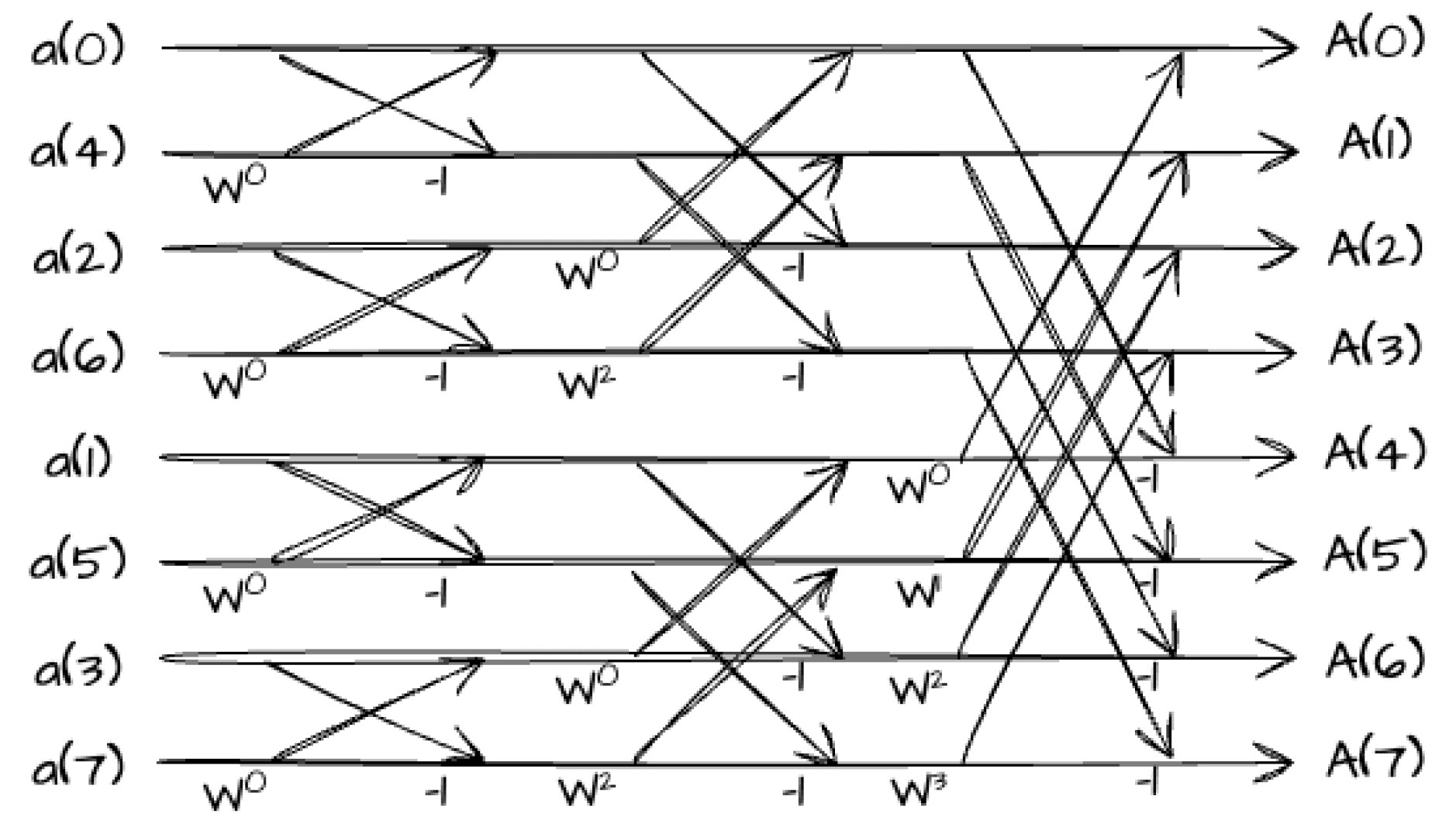
Figure 3. Sub-NTT Architecture.
2¹² NTT Architecture
The 2¹² NTT module consists of:
2x 64-point NTT modules,
1x point-wise multiplication module,
1x 64x64-point transpose module,
where the 64-point NTT module can be decomposed similarly to the 2¹² NTT, as the zoom-in figure presents below:
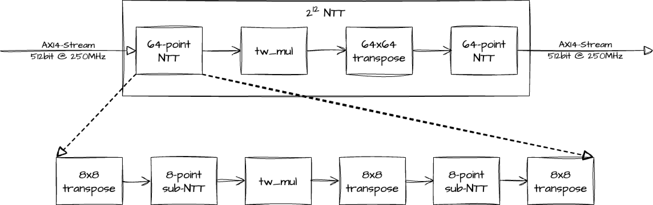
Figure 4. 2¹² NTT Architecture.
The 8x8 transpose module has the lowest memory requirement of 8x8x64 bit = 512 B, which easily fits in registers. The 64x64 transpose module requires at least 64x64x64 bit = 32 kB size of memory. Considering the size of a single BRAM module is 36 kbit (in total, 70.9 Mbit of on-chip BRAM is available), it is suitable to store the data in BRAM. Furthermore, a double-buffer architecture is adopted in the transpose module to achieve full pipelining, which requires 2x size of the least memory requirement.
2¹⁸ NTT Architecture
The 2¹⁸ NTT module consists of:
1x 64-point NTT module,
1x point-wise multiplication module,
1x 64x64x64-point transpose module,
1x 2¹² NTT module,
1x 64x64-point transpose module.
The 2¹⁸ NTT module could be interpreted as the extension of the 2¹² NTT module, as presented in the figure below:
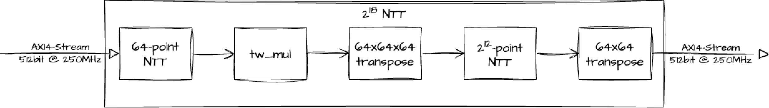
Figure 5. 2¹⁸ NTT Architecture.
The 64x64x64-point transpose can be composed of one 4096x64-point transpose and one 64×64-point transpose. This transpose module at least requires 64⁴ bit = 2 MB size of memory. The size of a single URAM module is 288 kbit (in total, 270 Mbit of on-chip URAM available), so we adopt URAM to store the data.
2²⁴ NTT Architecture
The 2²⁴ NTT module consists of:
2x 2¹² NTT modules,
1x point-wise multiplication module,
1x 2¹²x2¹² transpose module.
Inside the point-wise multiplication module, the twiddle factors are generated internally on the fly, which saves a lot of memory resources otherwise required for storing them. In addition, the 2¹² x 2¹² transpose module requires HBM resources and we interface it with 4x AXI4 interfaces (2x RD and 2x WR ports), as the zoom-in figure below indicates:
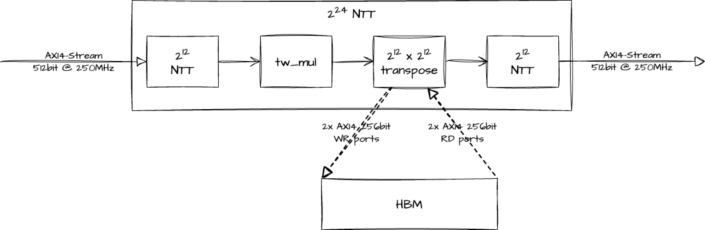
Figure 6. 2²⁴ NTT Architecture.
The HBM RD burst access is trivial since the read addresses are adjacent. To achieve HBM WR burst access, a URAM-based pre-HBM buffer is provided. This buffer is designed to perform a small-size pre-transpose, which ensures that the WR burst data is going to fit contiguous addresses.
Performance Report
In order to perform the hardware tests, we implement presented NTT module on AMD/Xilinx U55C FPGA board that features:
AMD/Xilinx VU47P FPGA
2x PCIe Gen4 x8
16 GB HBM
Total of 6x U55C FPGA boards are hosted inside our Gen1 server, and has the following specifications:
Lenovo SR655 server
AMD 7313P 16C 3.0 GHz 150 W
256 GB TruDDR4 3200 MHz
6x PCIe Gen4 x16 slots
Redundant 1600 W PSU
Latency
In order to precisely analyze latency, we perform hardware timestamping within the FPGA, as presented in the figure below. The timestamps are captured when input traffic hits the NTT module (T₀) and when the output traffic leaves it T₁. The latency values (T₁ - T₀) are stored in the Control and Status Register (CSR) bank and the CPU can read them out after the each executed test.
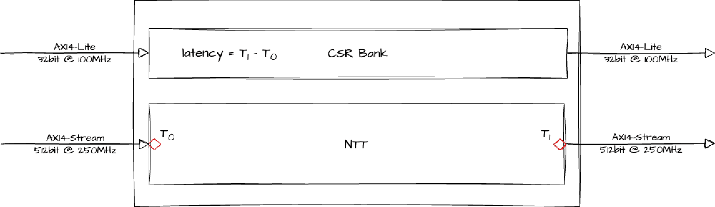
Figure 7. HW Timestamping within FPGA.
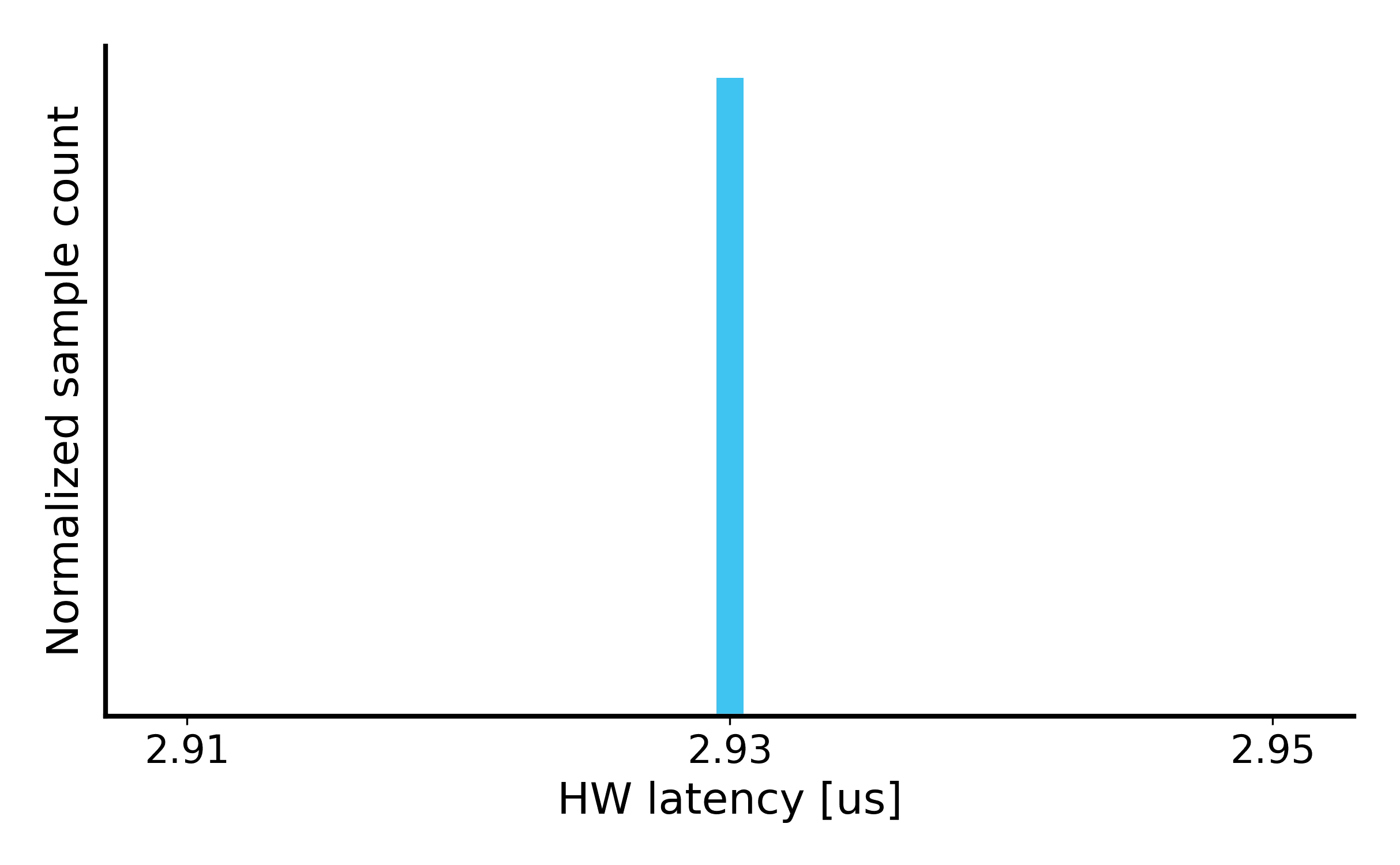
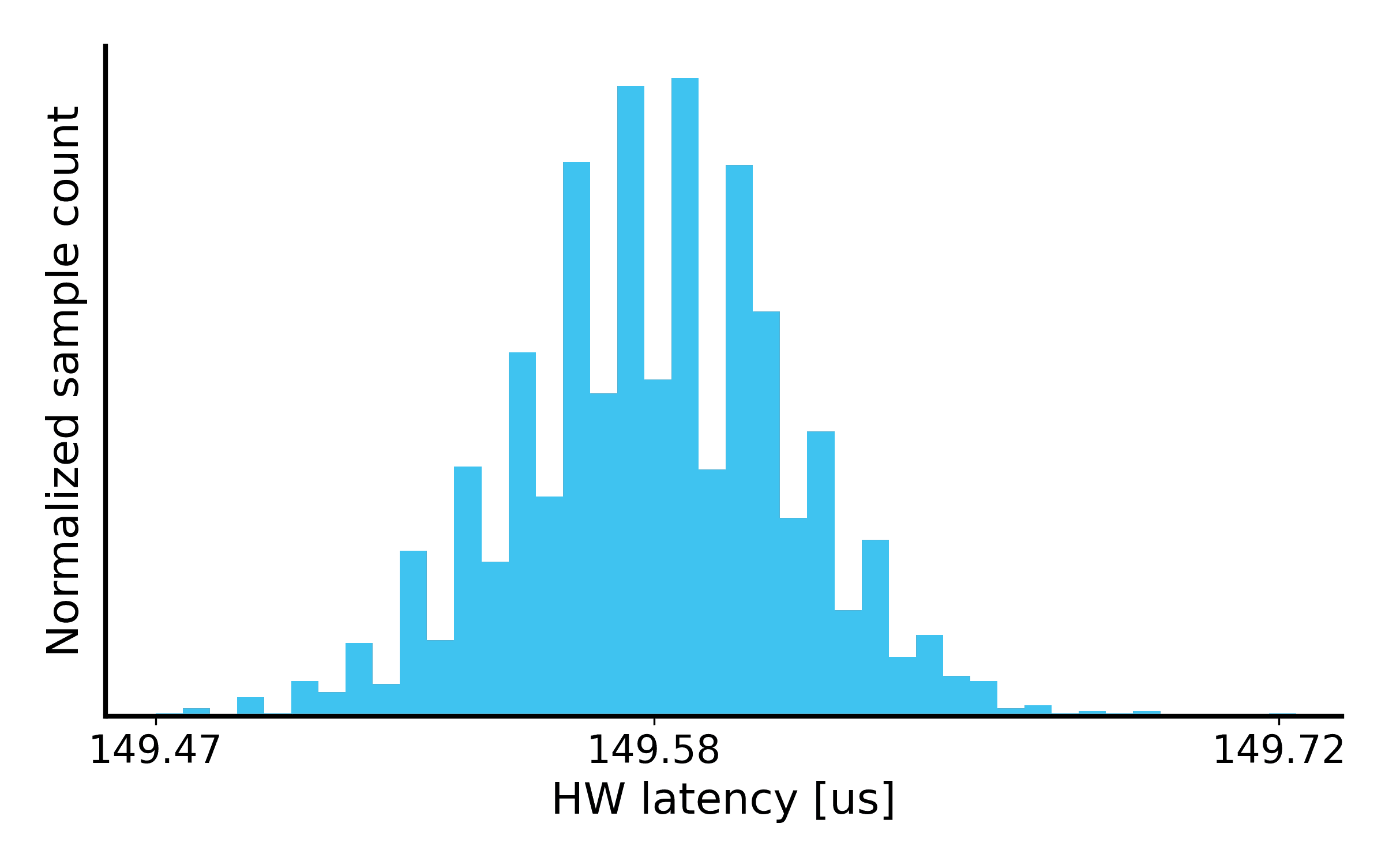
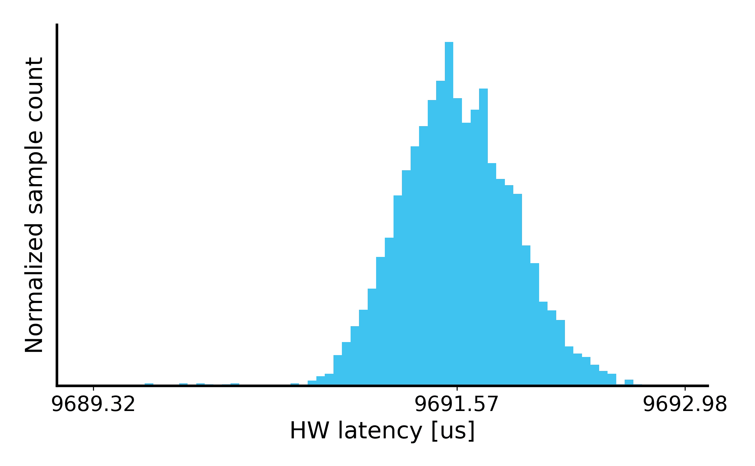
We report minimal (min), mean (avg), maximal (max) and median (med) latency in Table 1.
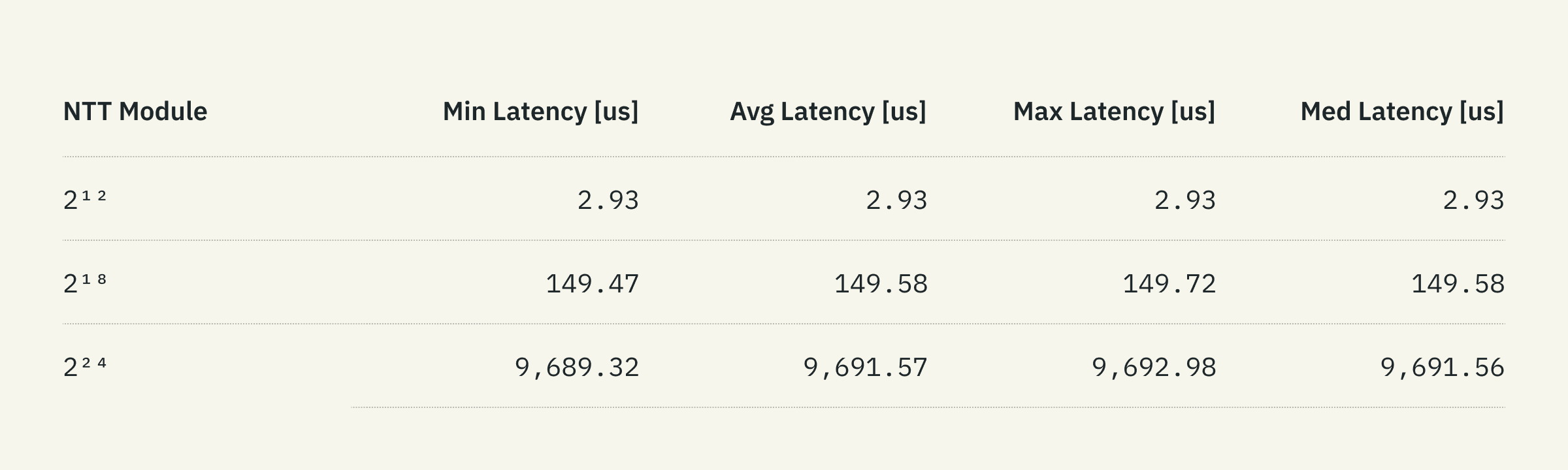
We discuss latency distributions for all three NTT modules:
2¹²: We observe constant latency which is explained by CPU’s ability to efficiently readout PCIe traffic. From the NTT module perspective, the PCIe TX FIFO is always available to NTT module to write to it hence there is no back-pressure. Normalized latency distribution is shown below:
2¹⁸: We observe an effectively unimodal latency distribution. The latency variance is caused by the sporadic PCIe TX FIFO back-pressure caused by the TLP construction and PCS 128b/130b encoding.
2²⁴: The HBM module has a non-deterministic latency profile due to the RD/WR access context switching and DRAM refresh cycles. The lower peak of the latency distribution occurs when WR burst is not back-pressured by the HBM refresh, while the higher peak of the latency distribution occurs when the WR buffer is back-pressured. The lower latency operation occurs more frequently which suggests that the URAM-based pre-HBM buffer significantly improves the performance.
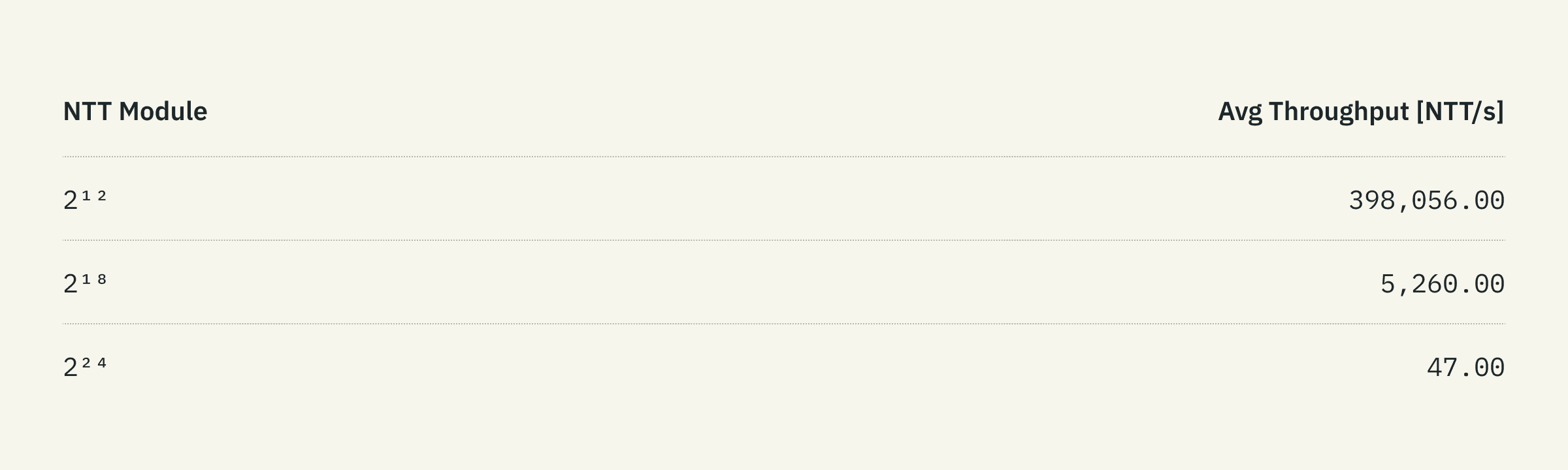
Throughput
We measure NTT compute throughput from the SW perspective, since that is a realistic ZKP acceleration scenario in production. Our SW stack does its best effort to push as many NTT computations as possible via the PCIe to the FPGA. While the theoretical throughput for the PCIe Gen4 x8 lanes is 128 Gbps, we are capable of achieving approximately 100 Gbps for 2¹² NTT computations. For NTT sizes greater than the L3 cache size of 128 MB, the CPU performs constant cache fetches while computation inputs are sent to the PCIe, resulting in reduced throughput of approximately 50 Gbps for 2²⁴ NTT computations.
Power Consumption
We measure the total power server consumes and report values that reflect the power consumption of an FPGA running the NTT module. The baseline power consumption of an idle server is 110 W. It is important to indicate that the standard PCIe slot power consumption is limited to 75 W and we are hitting it in our size- 2²⁴ tests. We are not providing PCIe Aux Power supply which is required for more power-hungry HW modules.
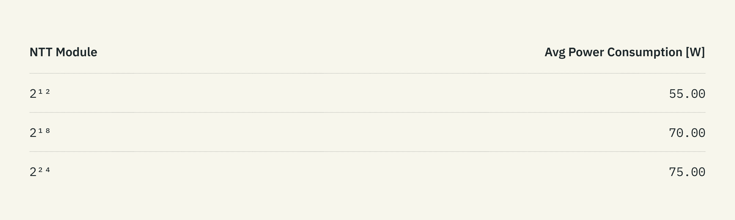
Power consumption is strongly dependent on the system clock which runs at 250 MHz for each NTT module. Larger NTT modules consume more power since there is more digital logic involved but also more memory, especially for the 2²⁴, which utilizes the HBM.
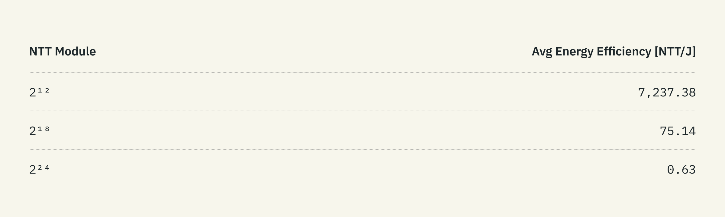
Energy Efficiency
Energy efficiency is the key performance metric since it defines the baseline costs of the NTT, and associated ZKP, computations. It combines computation throughput [NTT/s] and power consumption [W]. Since the power/time [Ws] product is energy [J], the energy efficiency is often reported in [NTT/J].
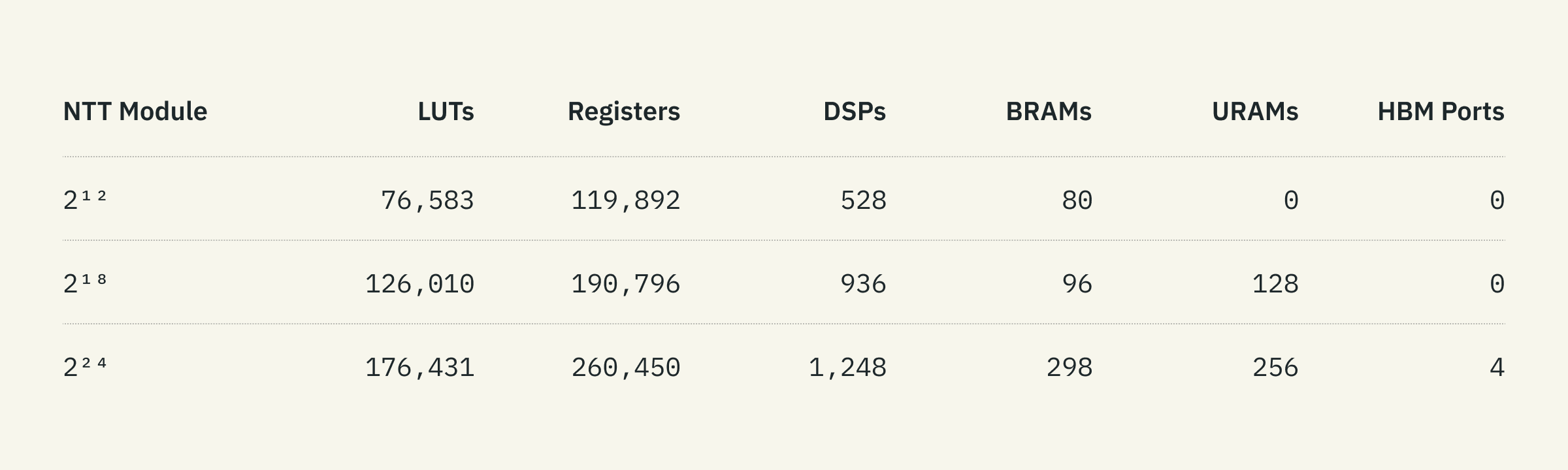
Resource Utilization
The following resource utilization is reported per single NTT module. The figures represent only the NTT core utilization and do not provide insights into additional resources used, such as the PCIe HW controller for example.
Case Study: Accelerating Low-Degree Extension for Polygon zkEVM
We now demonstrate the application of our acceleration architecture to a real-world cryptographic system: Polygon zkEVM, which is set to launch in late March 2023 as the first Layer-2 zkEVM on Ethereum. A significant portion of the overall computation of batch proofs is the GL64 Low-Degree Extension (LDE) module. An LDE is a sequence consisting of an INTT over a smaller vector followed by an NTT on the result, padded to a larger vector length.
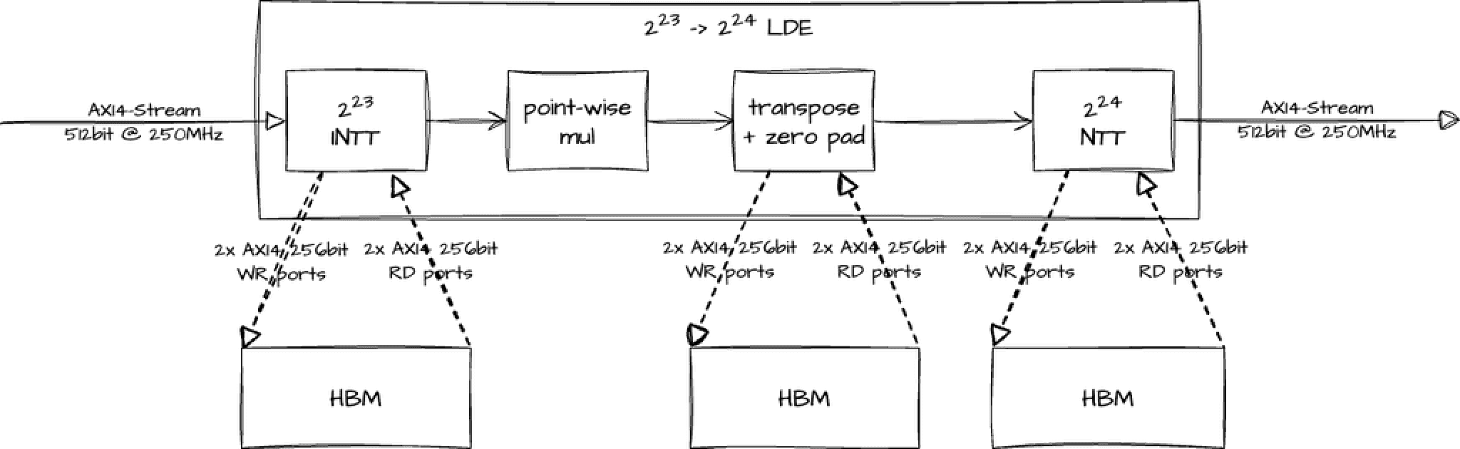
Figure 8. 2²³ → 2²⁴ LDE Architecture.
We utilize this GL64 NTT design to accelerate the Polygon zkEVM prover and provide a detailed performance report of GL64 2²³ → 2²⁴ LDE module running on our Gen1 server. The measurements reported are per FPGA, and each server in our Gen1 cluster hosts 6x AMD/Xilinx U55C FPGA cards.
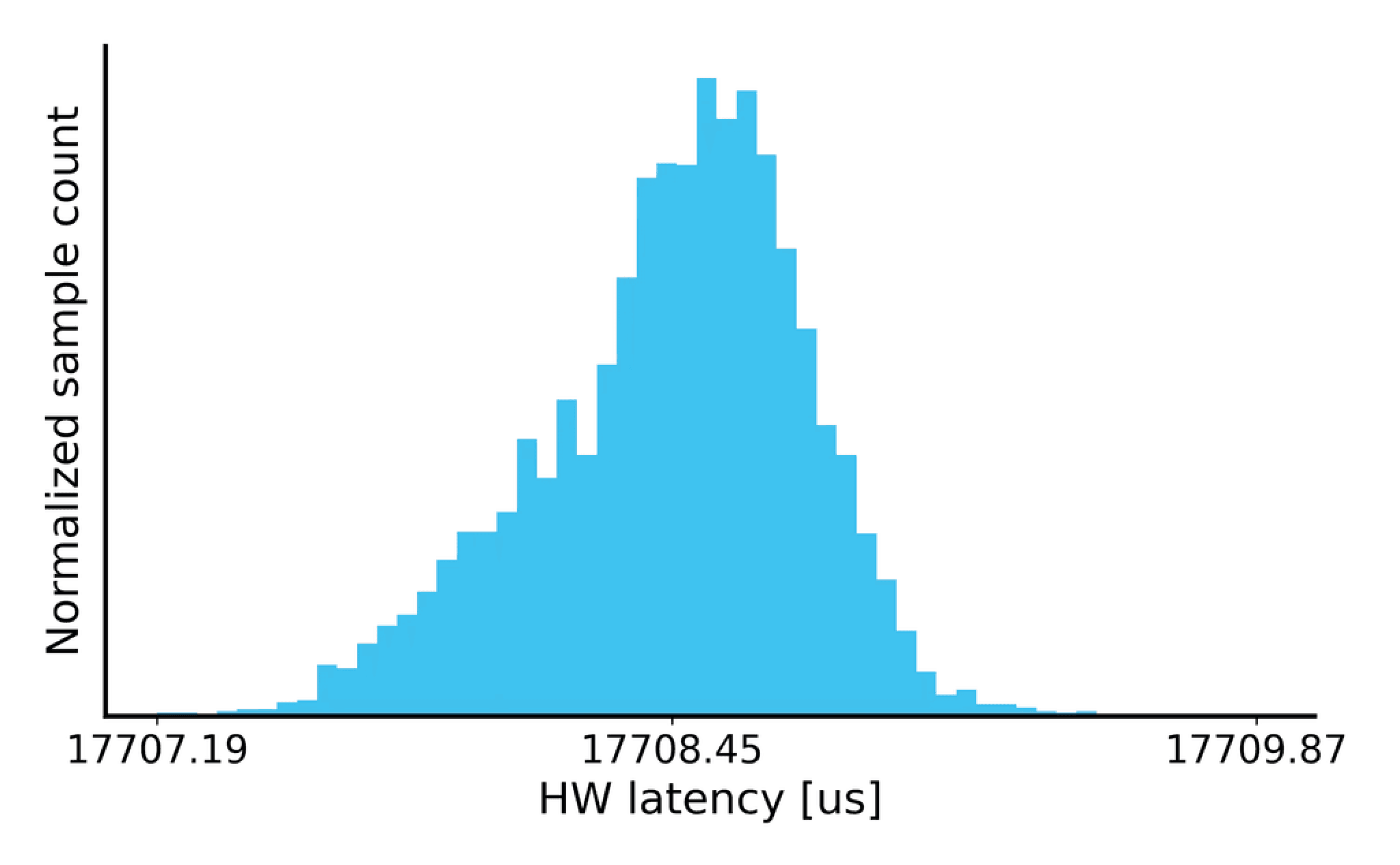
Latency
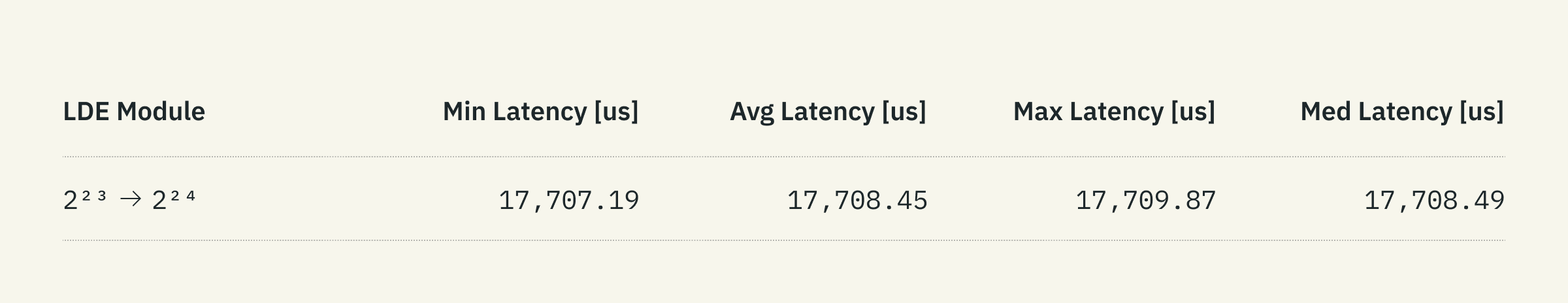
The LDE module has a non-deterministic latency profile due to three internal HBM modules. Each HBM module has its own lower- and higher-latency operation caused by the RD/WR access context switching and DRAM refresh cycles. The final LDE latency profile is a superposition of the three non-deterministic latency profiles.
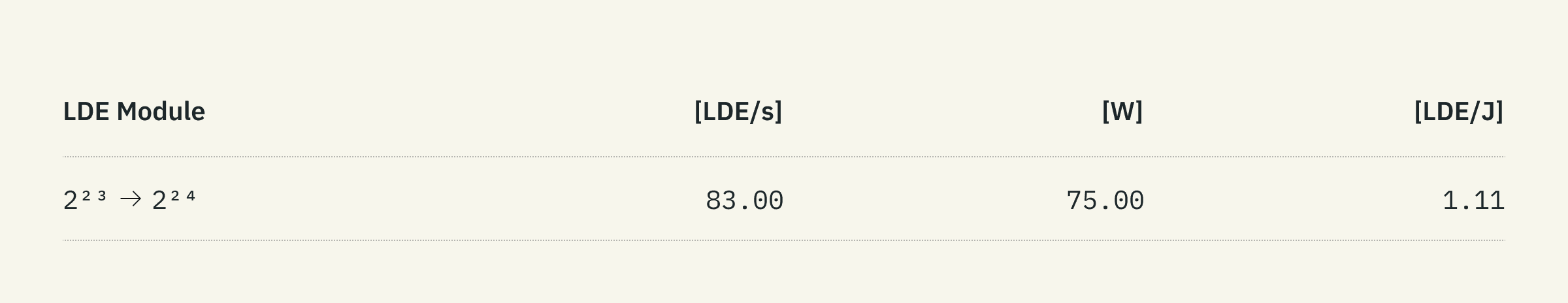
Throughput / Power Consumption / Energy Efficiency
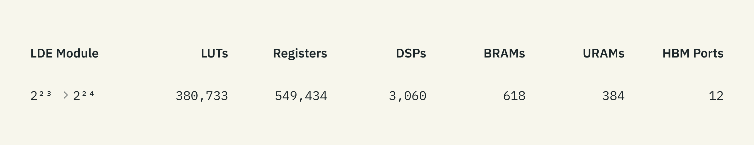
Resource Utilization
Performance Comparison to the AWS c6i Instance
We are reporting a performance comparison to the official software implementation of 2²³ → 2²⁴ LDE used by Polygon zkEVM. The largest single batch of LDE operations in the Polygon zkEVM batch proof computation at the time of writing is 665 vectors at a time, performed in the first round of the STARK protocol. We compare our performance with software benchmarks run on a 128-vCPU AWS c6i.metal instance, the latest compute-optimized instance with the x86_64 architecture available from the cloud provider. Our Gen1 server accelerates 665x LDE operations using 6x FPGAs in parallel, achieving total throughput of 498 LDE/s (for 83 LDE/s per FPGA). The performance comparison is presented in the table below:
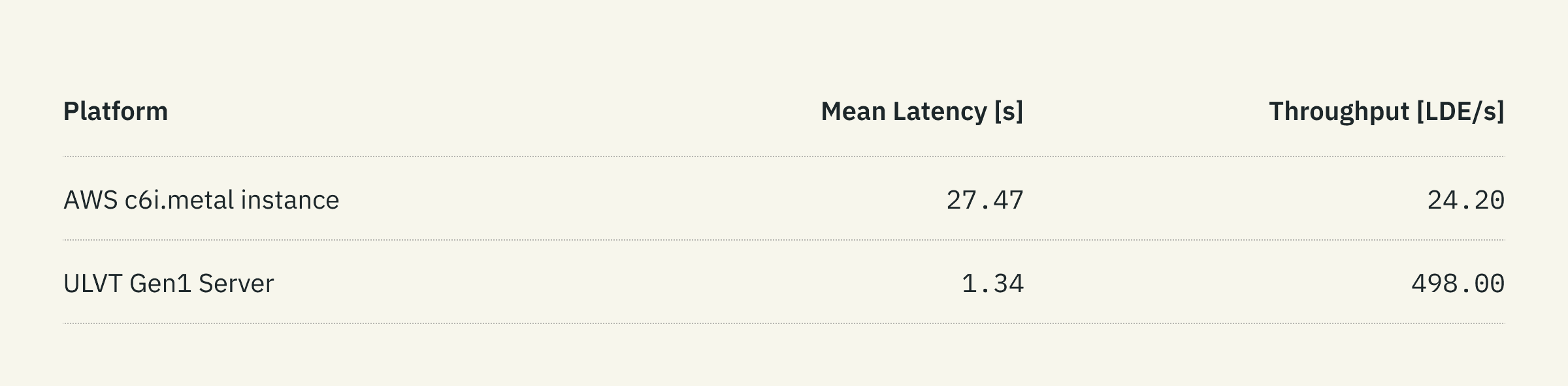
We are very excited to report that the processing time is reduced from 27.47s to 1.34s (~20x).
Conclusion
Our conviction at Ulvetanna is that hardware acceleration is a crucial in enabling ZKPs to scale for real-world use cases. Where many projects are focused narrowly on the problem of reducing latency of computation, our results demonstrate the performance attainable with an FPGA server specially designed for high-throughput and energy-efficiency.
The introduction of HBM for FPGAs is essential for large NTTs because it allows us to perform large transposes within the accelerator, and PCIe Gen4 allows for the design of higher throughput pipelined architecture. With the GL64 field seeing increased usage in ZKP projects across the industry, we hope this report serves as additional testament to the efficiency NTT-heavy protocols can see with this particular choice of field.